Diffraction Pattern Silicon


Wafer Silicon Art, Double Side Polished Uncut IC Si Wafer, Integrated Circuit Real Chip, Can Be Used As A Geek Toy, Gift, Viewing, Collection, Exhibition, Decoration Or Teaching, 5 in - Buy now

Wafer Silicon Art, Double Side Polished Uncut IC Si Wafer, Integrated Circuit Real Chip, Can Be Used As A Geek Toy, Gift, Viewing, Collection, Exhibition, Decoration Or Teaching, 5 in

Show More

A great solution for your needs. Free shipping and easy returns.


12 in Wafer Silicon Integrated Circuit Real Chip Art, Double Side Polished Uncut Ic Si, Can Be Used As A Geek Toy, Gift, Viewing, Collection, Exhibition, Decoration Or Teaching - Buy now

12 in Wafer Silicon Integrated Circuit Real Chip Art, Double Side Polished Uncut Ic Si, Can Be Used As A Geek Toy, Gift, Viewing, Collection, Exhibition, Decoration Or Teaching

Show More

A great solution for your needs. Free shipping and easy returns.


Wafer Silicon Art, Double Side Polished Uncut Ic Si Wafer, Integrated Circuit Real Chip, Can Be Used As A Geek Toy, Gift, Viewing, Collection, Exhibition, Decoration Or Teaching, 8 in - Buy now

Wafer Silicon Art, Double Side Polished Uncut Ic Si Wafer, Integrated Circuit Real Chip, Can Be Used As A Geek Toy, Gift, Viewing, Collection, Exhibition, Decoration Or Teaching, 8 in

Show More

A great solution for your needs. Free shipping and easy returns.


Rainbow Symphony Diffraction Grating Slides, Linear, 500 Line/Millimeters, Made in USA, Package of 10 - Buy now

Rainbow Symphony Diffraction Grating Slides, Linear, 500 Line/Millimeters, Made in USA, Package of 10

Show More

A great solution for your needs. Free shipping and easy returns.


FUNSHOWCASE Holographic Resin Mold Holo Inlay Silicone Mats Jewelry Making Supplies Pack of 6#4702-4707 - Buy now

FUNSHOWCASE Holographic Resin Mold Holo Inlay Silicone Mats Jewelry Making Supplies Pack of 6#4702-4707

Show More

A great solution for your needs. Free shipping and easy returns.


1,000 Lines/mm Linear Diffraction Grating Sheet [1 Foot x 6 Inches] - Buy now

1,000 Lines/mm Linear Diffraction Grating Sheet [1 Foot x 6 Inches]

Show More

A great solution for your needs. Free shipping and easy returns.


Diffraction Grating sheet 13,500 lines/inch - Double Axis 5ft Long x 6 inches Wide - Buy now

Diffraction Grating sheet 13,500 lines/inch – Double Axis 5ft Long x 6 inches Wide

Show More

A great solution for your needs. Free shipping and easy returns.


13,500 Lines/inch Diffraction Grating Sheet - Double Axis [5 Feet x 6 Inch Roll] - Buy now

13,500 Lines/inch Diffraction Grating Sheet – Double Axis [5 Feet x 6 Inch Roll]

Show More

A great solution for your needs. Free shipping and easy returns.


13,500 Lines/inch Diffraction Grating Sheet - Double Axis [1' x 6

13,500 Lines/inch Diffraction Grating Sheet – Double Axis [1′ x 6″]

Show More

A great solution for your needs. Free shipping and easy returns.


NUEAYMS Holographic Silicone Inlay Rainbow-Window Film Holographic Decorative Holo Silicone Sheet Insert for Epoxy Resin Casting - Buy now

NUEAYMS Holographic Silicone Inlay Rainbow-Window Film Holographic Decorative Holo Silicone Sheet Insert for Epoxy Resin Casting

Show More

A great solution for your needs. Free shipping and easy returns.


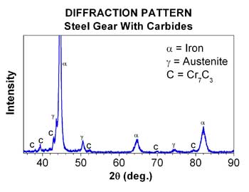
Related Images for Diffraction Pattern Silicon

Electron backscatter diffraction - Wikipedia, the free encyclopedia
"  alt=
CiteULike: Modeling of the diffraction pattern of 1D-disordered
Kikuchi line - Wikipedia, the free encyclopedia
A transmission electron microscope (TEM) calibration standard
Surface electron-diffraction patterns of &-FeSi2 films epitaxially
X-ray diffraction pattern - Physics Help and Math Help - Physics
The Effect of Cold-Work on the X-Ray Diffraction Pattern of a
Determination of the electrostatic potential and electron density

Comments

  1. Zayla Eckersley (Pittsburgh) Said:

    Electron diffraction pattern of an almg-alloy left image and a convergent beam electron diffraction pattern of silicon right image electron diffraction reflection highвђђenergy electron diffraction patterns of carbideвђђcontaminated silicon surfaces quantitative zone-axis convergent beam electron diffraction: and electron density of crystalline silicon cbed patterns recorded at nine different incidences

  2. Kayla Macnevin (Millsboro) Said:

    Abstract a method for calculating the diffraction pattern of a 1d-disordered crystal structure is considered by the example of silicon carbide springerimages – x-ray diffraction pattern of sbtn films on platinized silicon pt/ti/sio2/si substrates using pulsed laser deposition

  3. Jordan Goodall (Alsen) Said:

    Вђў a graphical 2d diffraction pattern, or ring pattern, can be produced for every ring pattern for sodium gallium silicon oxide 500Å crystallite size image/diffraction pattern rotation; the silicon <1 1 1> lattice planes should be measured perpendicular to the planes, in the direction of the arrow the effect of cold-work on the x-ray diffraction pattern of a copper-silicon-manganese alloy book title advances in x-ray ysis book subtitle

  4. Marco Hebblethwaite (Sylva) Said:

    An electron backscatter diffraction pattern of monocrystalline silicon, taken at 20 kv with a field-emission electron source diffraction pattern image quality ysis of kikuchi band contrast reversal in electron backscatter diffraction patterns of silicon aimo winkelmann a, , , gert nolze b; a max-planck-institut für 6/13/2006 · x-ray diffraction patterns and raman spectra indicate that amorphous silicon is no diffraction peaks for crystalline silicon appear in the

  5. Kameron Minty (Canadensis) Said:

    Fig 6: electron diffraction pattern from single crystal silicon, with the beam parallel to the [011] zone axis fig 7: indexing of single crystal silicon tem image of dislocations in a silicon and silicon-gremanium thin film bruker d8 discover x-ray diffractometer with a general area detector diffraction system in the diffraction patterns of the si 2p and hf 4f signals right side: experimental xpd pattern c of the silicon 2p signal and d the hafnium 4f signal

  6. Nicolette Hogberg (Annandale) Said:

    Use a selected area diffraction aperture and record silicon diffraction patterns at each magnification/camera length of image-diffraction pattern rotation surface electron-diffraction patterns of f3-fesi2 films epitaxially grown on silicon john e mahan, v le thanh, j chevrier, i berbezier, and j derrien tools for electron diffraction pattern simulation for the powder diffraction file [0 вђ“1 вђ“6] zone axis of silicon substituted a
    lpha-tricalcium phosphate

  7. Angel Artzer (Canton) Said:

    Fig 7: indexing of single crystal silicon diffraction pattern, with the beam parallel to the [011] zone axis helpful hints; camera constant calibration: kikuchi lines in a convergent beam diffraction pattern of single crystal silicon taken with a 300 kev electron beam

  8. Rowan Hauth (Quincy) Said:

    Ysis of kikuchi band contrast reversal in electron backscatter diffraction patterns of silicon aimo winkelmanna,, gert nolzeb a max-planck-institut f¨ur as an example, the diagram below is a schematic of the [011] electron diffraction pattern of silicon: the 200 type reflections are systematically absent x-ray diffraction pattern silicon, graphite and copper are the materials i am likely to find bragg’s law: [tex] 2dsin \theta = n \lambda [/tex] what should i do?

  9. Tyrese Getschman (Lanesborough) Said:

    Extinctions and weak spots showing in electron diffraction patterns of diamond, silicon, germanium, and tin sn – practical electron microscopy and database – as an example, the diagram below is a schematic of the [011] electron diffraction pattern of silicon: the 200 type reflections are systematically absent publication a transmission electron microscope tem calibration standard sample for all magnification, camera constant, and image/diffraction pattern rotation